Professional
Leading
![[LOGO]](http://www.cotonix.com/en/template/default/image/logob.png)
![[LOGO]](http://www.cotonix.com/en/template/default/image/logoll.png)
Professional
Leading

Reliability Guarantee
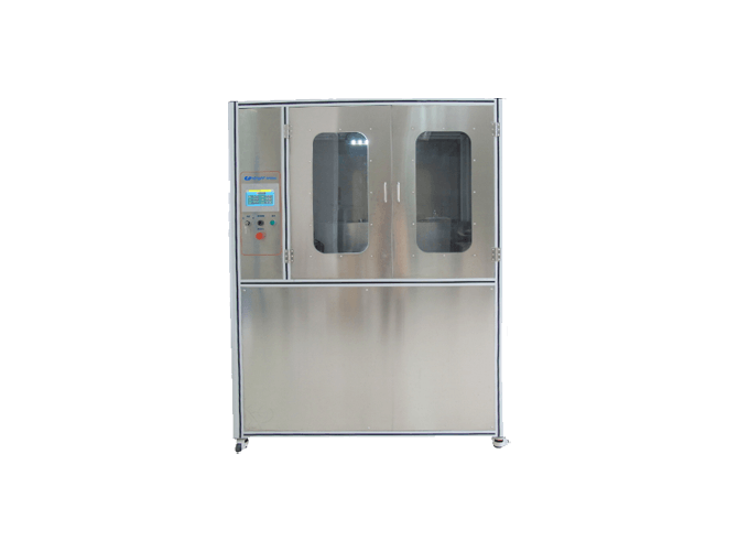
Total Cleaning Process Solution Provider
 Enquire Now
![[x]](/en/template/default/picture/closeicon1.png) Enquire Now
Enquire Now
Enquire Now
Enquire Now
![[→]](/en/template/default/image/zixuniconim1.png) Enquire Now
Enquire Now
![[x]](/en/template/default/image/closeicon1.png)
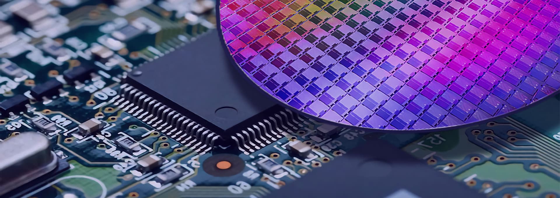
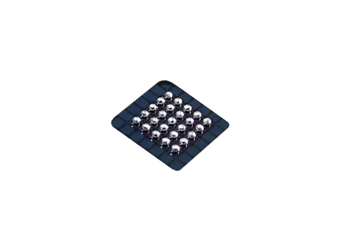
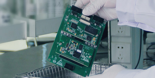
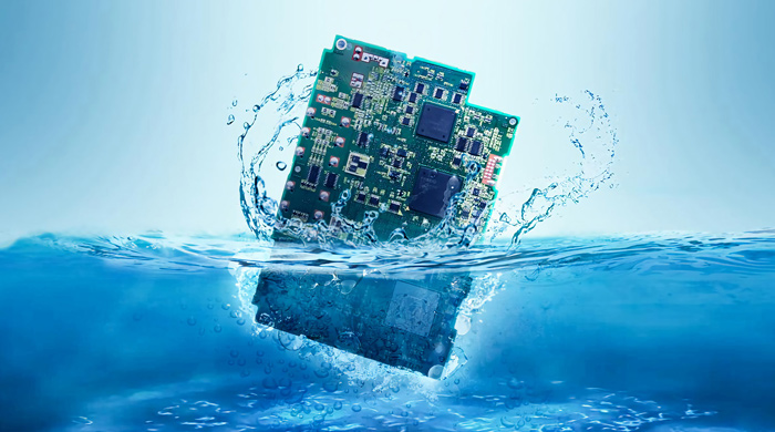
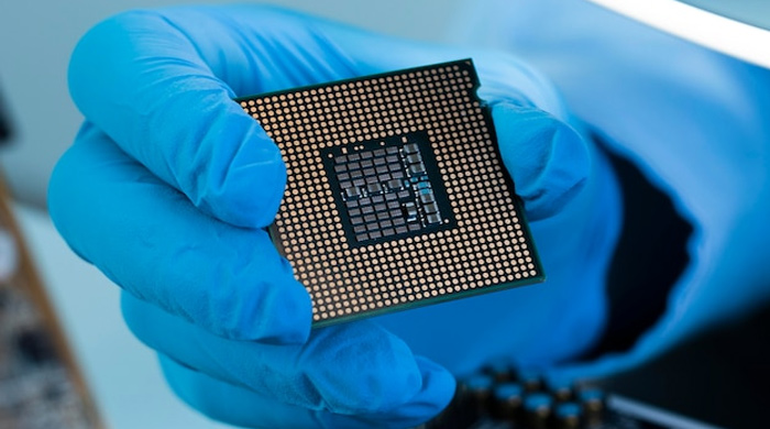
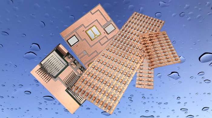
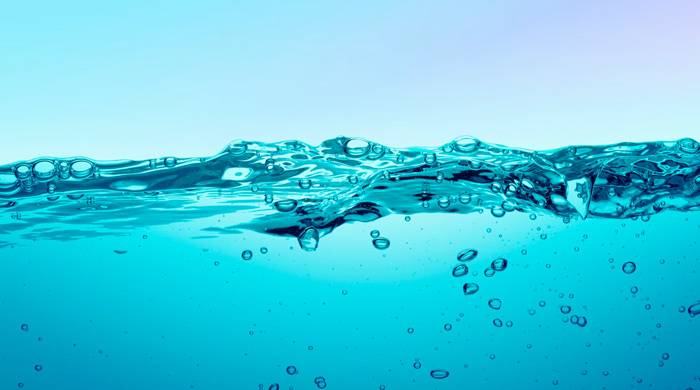
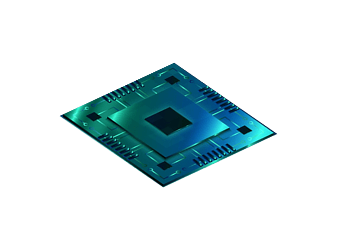
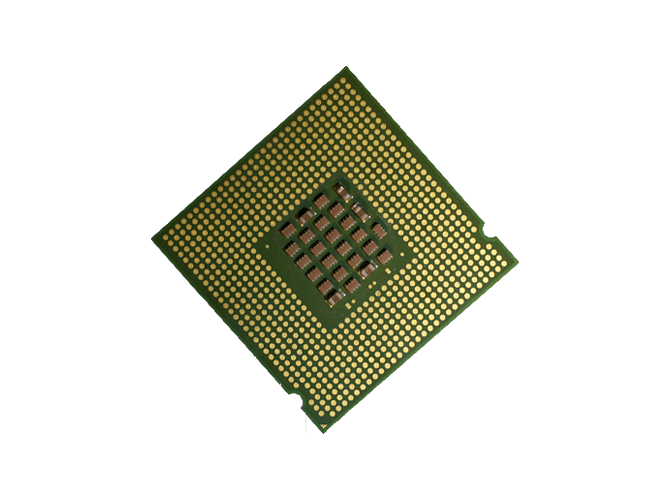
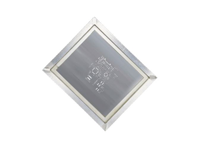
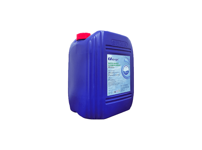
In response to the different requirements for precise post soldering cleaning of advanced packaging product chips, substrate pads, and electronic processes before soldering, Unibright has independently developed a relatively complete water-based series of products, covering from semiconductor packaging to PCBA component terminals, including water-based and semi water-based cleaning agents, alkaline water-based cleaning agents, and neutral water-based cleaning agents. Specifically, under the same cleaning force, Unibright's cleaning agents have good compatibility, a wider range of compatible materials, faster cleaning speed, low ion residue, and better cleanliness.
![[x]](/en/template/default/picture/closeimgfz1.svg)

![[→]](/en/template/default/picture/you.svg)


![[↓]](/en/template/default/image/xiangxiaimgfaz1-1.svg)


![[ico]](/en/template/default/picture/fc1c83eb02c951ce168aaebde4fd8205.svg)


![[↑]](/en/template/default/picture/rtxiangshangimg1.svg)